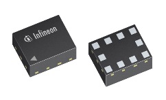
BGS12PN10E6327XTSA1


L'image affichée est une représentation non contractuelle
Download the free Library Loader to convert this file for your ECAD Tool
- Polarity
- CMOS
- Frequency f
- 900 MHz
- Package
- TSNP-10
- Automotive
- NO
- RoHS Status
- RoHS-conform
- Packaging
- REEL
- Référence fabricant
- SP001197200
- ECCN
- EAR99
- Numéro du tarif douanier
- 85423990000
- Pays
- Malaysia
- Annuaire ABC
- B
- Délai de livraison standard
- 14 Semaines
The BGS12PN10 is a Single Pole Dual Throw (SPDT) high linearity, high power RF switch optimized for mobile phone applications up to 6.0 GHz. This single supply chip integrates on-chip CMOS logic driven by a simple, CMOS or TTL compatible control input signal. Unlike GaAs technology, the 0.1 dB compression point exceeds the switch maximum input power level, resulting in linear performance at all signal levels and external DC blocking capacitors at the RF ports are only required if DC voltage is applied externally.
The BGS12PN10 enables critical band combinations for UL (B1 + B3), (B2+B4), DL-CA (B4 + B12) and SV-LTE (B5 + B13). This device handles very high transmitting signal levels of up to 38 dBm, while at the same time exhibiting low losses to conserve battery power. Ultra high linearity devices have a significant impact on system sensitivity. For instance, 3 dBm more linearity in whole RF-front-end leads to 6 dB better signal-to-noise ratio. Hence, data rate speed is improved by up to 40% allowing a step e.g. from 20 Mbps (QAM16 4/5) to 33 Mbps (QAM64 4/5). The BGS12PN10 stands for Best-in-Class ISO and IL performance across all frequencies.
Summary of Features
- High max RF power: 38 dBm
- Two ultra-low loss ports:
- 0.17 dB @ f=0.9 GHz, PIN=38dBm
- 0.22 dB @ f=1.9 GHz, PIN=38dBm
- 0.26 dB @ f=2.7 GHz, PIN=33dBm
- 0.37 dB @ f=3.6 GHz, PIN=33dBm
- 0.68 dB @ f=5.8 GHz, PIN=33dBm
- No DC decoupling components required, if no external DC is applied on RF ports
- High ESD robustness
- Low harmonic generation
- High linearity: 75dBm IIP3
- No power supply blocking required
- Supply voltage range: 1.8 to 3.6V
- No insertion loss change within supply voltage range
- No linearity change within supply voltage range
- 0.5 to 6.0 GHz coverage
- Small form factor 1.1 mm x 1.5 mm
- 400 µm pad pitch
- RoHS and WEEE compliant package
Potential Applications
- Suitable for EDGE / C2K / LTE / WCDMA / SV-LTE
- Mobile cellular Rx/Tx applications
- Optimized for main path and entire RF Front-end without any power restrictions in mobile communication:
- DL/UL CA and MIMO
- HPUE 26dBm devices (high power Tx)
- Micro/Pico Cells/Cellular Base stations
- Test equipment
Vous pouvez commander de manière définitive les articles du panier ou - si vous avez encore des questions - ou adresser celui-ci comme demande sans engagement.
Rutronik24 e-commerce est réservé exclusivement aux organisations et clients Corporates.
